
(주)코아시아세미
코아시아세미 PKG Design Engineer 채용
51-300명
경조금
복지포인트
음료/간식 제공
식대 지원
장기근속 포상
점심 제공
저녁 제공
임신/출산 지원
문화생활 지원
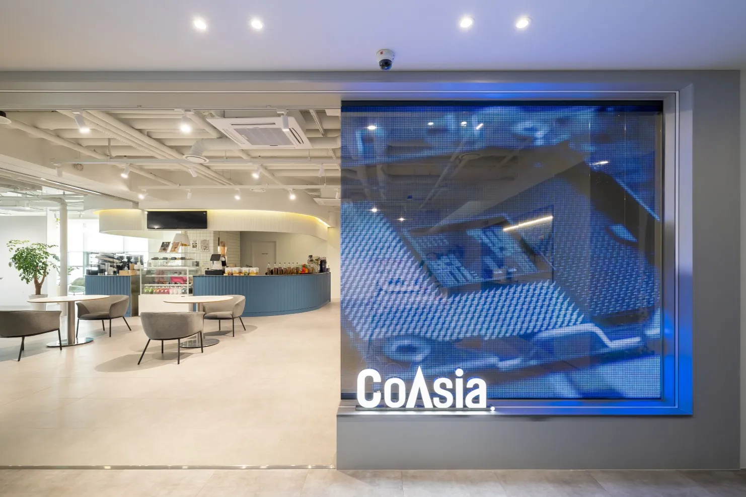
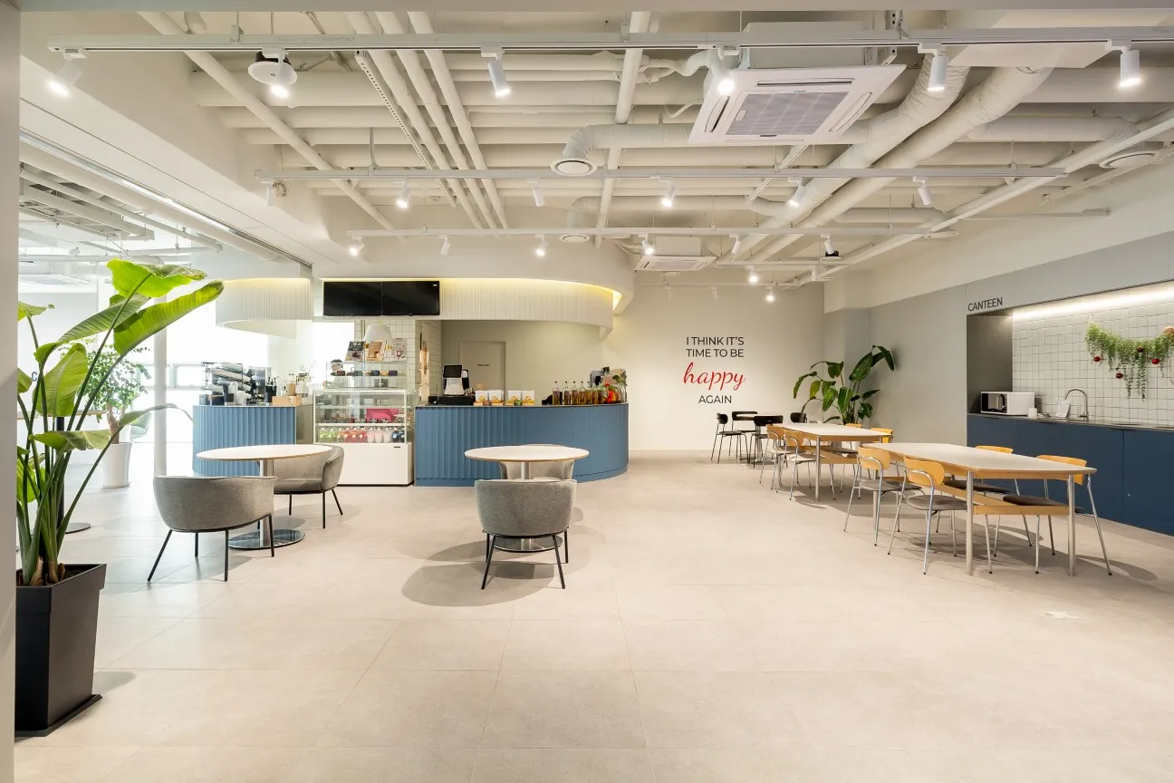
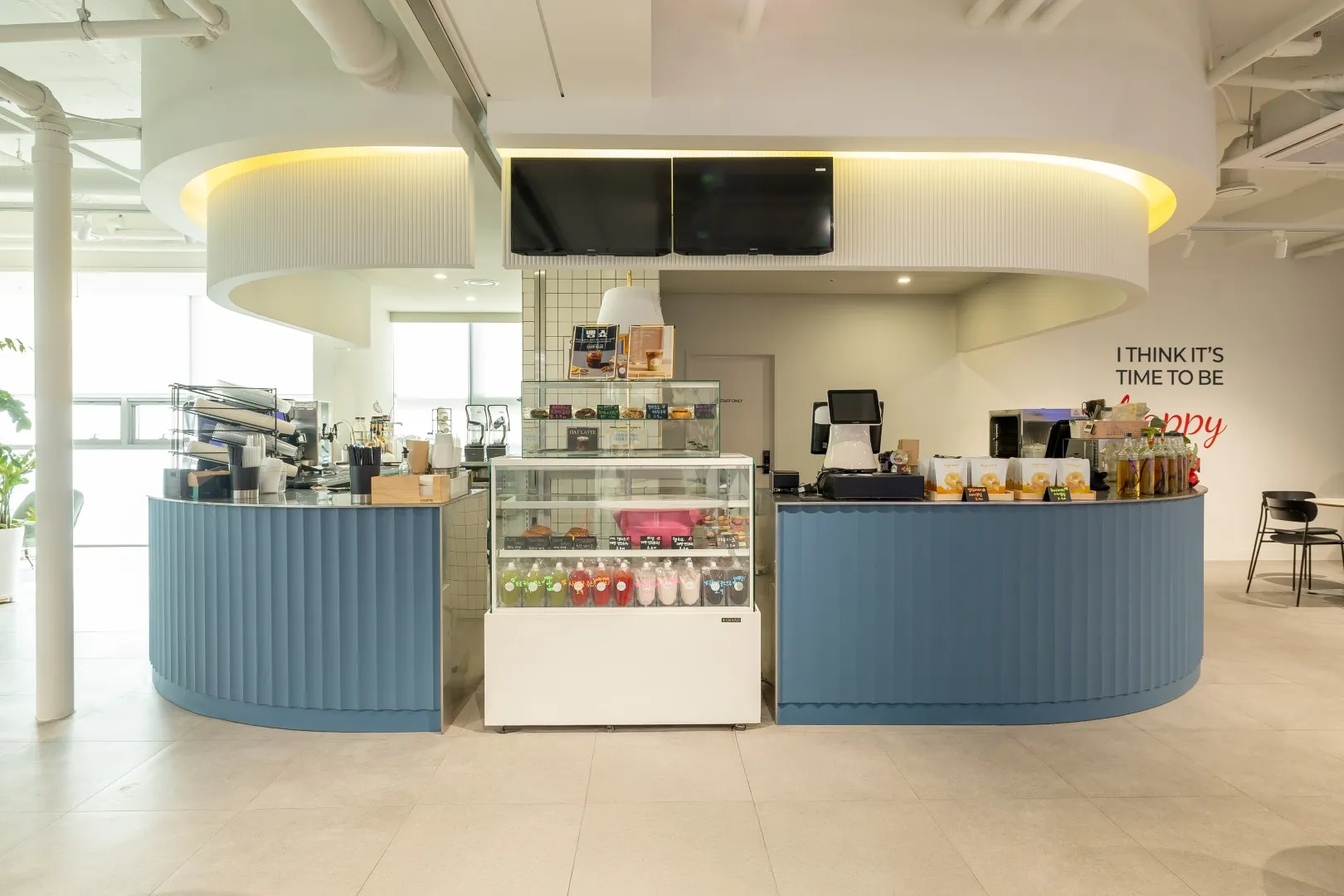
카페테리아
도서 구입비 지원
- 공고소개
- 주요업무
- 자격요건
- 우대사항
- 채용절차
- 기타안내
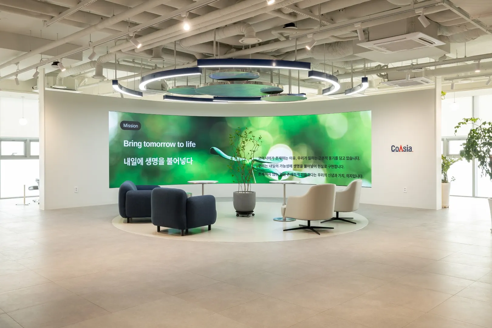
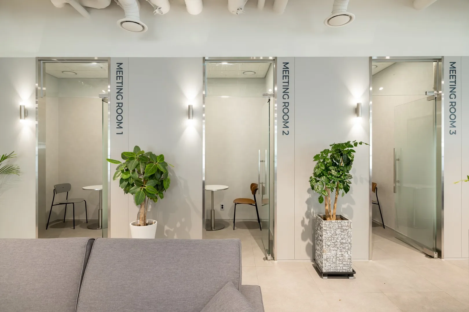
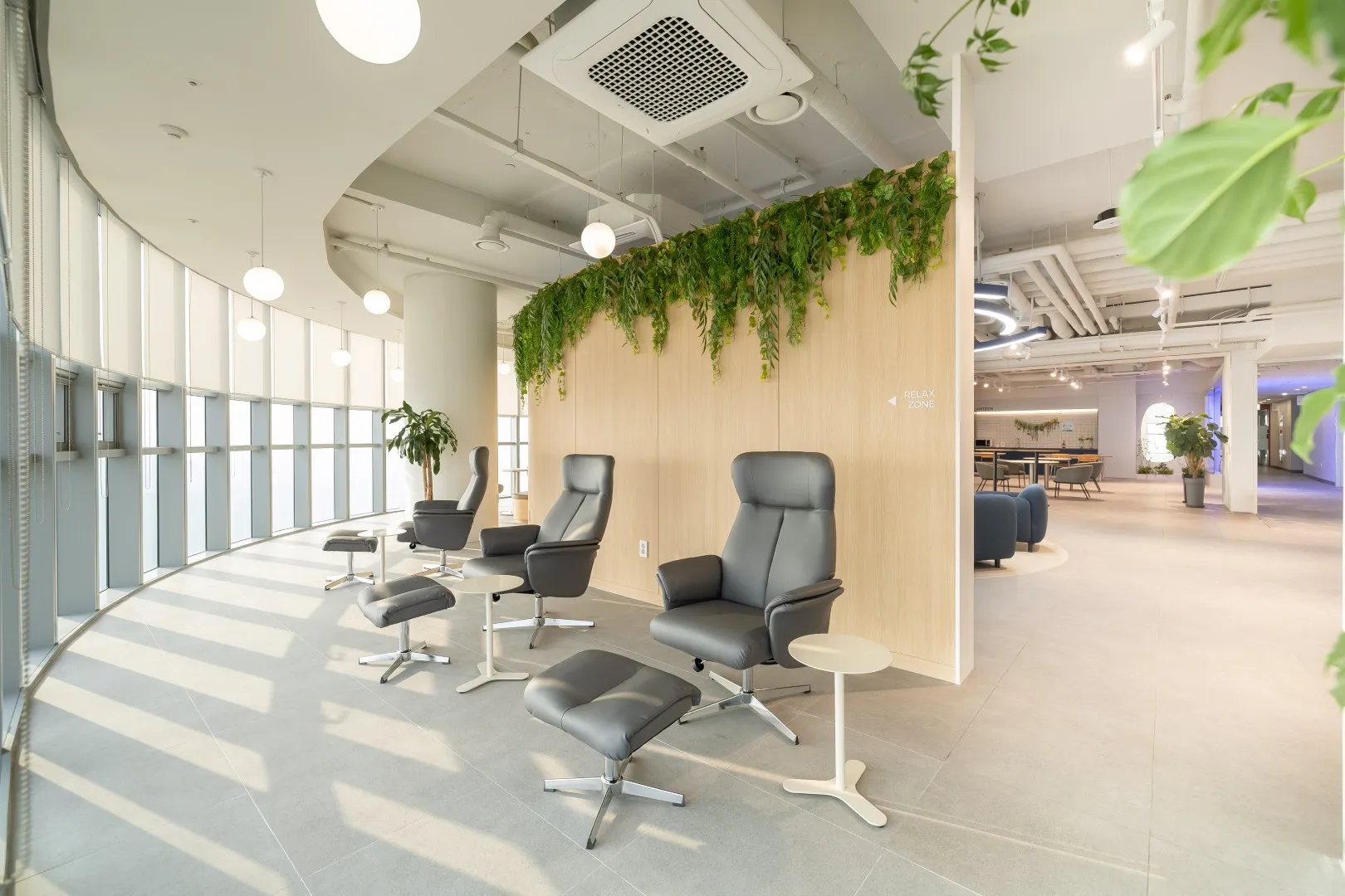
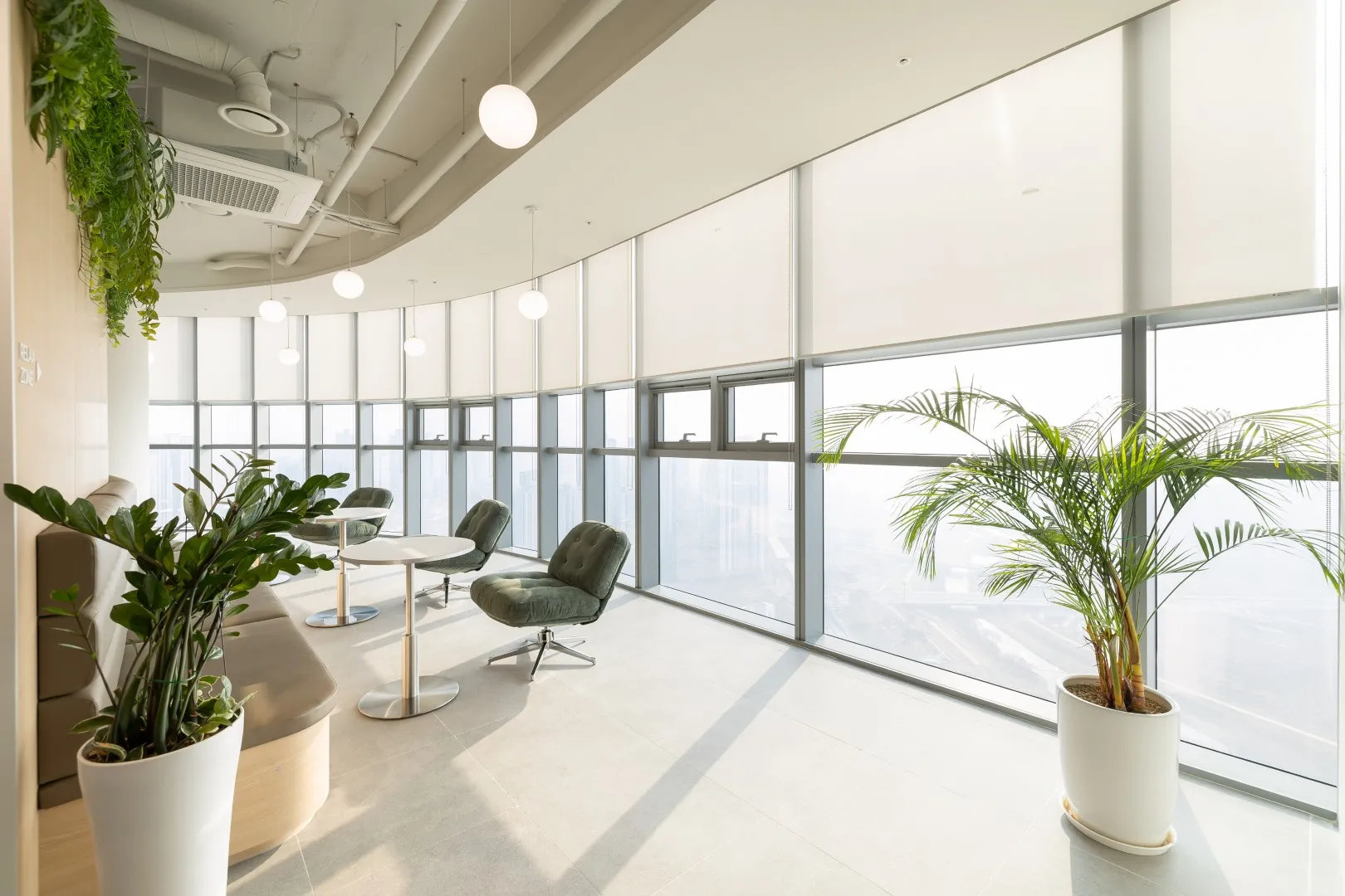
CoAsia SEMI는 혁신적이고 가치 있는 기술로 세상을 한 단계 더 발전시키고
고객과 함께 성장하는 글로벌 반도체 설계 전문 기업입니다.
사양 정의(Spec.)부터 RTL, Netlist, GDS까지 반도체 설계 전 공정을 아우르는
서비스를 제공하며, IP 커스터마이징, 설계 기술, 플랫폼 솔루션을 통해
고객 맞춤형 가치를 실현합니다.
또한 패키징, 테스트, 품질 관리를 포함한 턴키(Turnkey) 솔루션을 제공하는
토탈 솔루션 프로바이더로서, 반도체 개발 전 과정에 걸친 최적의 해법을 제시합니다.
CoAsia SEMI provides the best semiconductor design service for
all customers who make the world one step further with
innovative and useful technologies.
We offer a wide range of customer interfaces from Spec.
to RTL, netlist,and GDS.
We also offer IP customization, design technologies and platform solutions.
We serve as a Total Solution Provider that provides turnkey solutions
including package, test, and quality control.
주요업무
• Design FCCSP, FCBGA, and advanced semiconductor packages.
• Develop substrate layouts from die bump assignment to BGA ball-out.
• Perform package floor planning, layer planning, bump escape,
and substrate routing.
• Collaborate with SoC, SI/PI, thermal, mechanical, and test teams to
optimize package architecture.
• Review design rules, manufacturing capability,
and OSAT assemblyrequirements.
• Lead design reviews with customers, OSATs, substrate vendors,
and internal teams.
• Review and release package design data, including layouts, netlists,
stack-ups, and artwork.
• Support DFM, design verification, fabrication, assembly, and qualification.
• Manage package specifications, checklists, and release documents.
• Identify design risks and propose technical improvements.
자격 요건
• Bachelor's degree holders
• At least 2 years of relevant experience.
• Working proficiency of the English language and Korean (Preferred Korean)
우대사항
• 유관 부서 인력과 원활한 협업 가능자(회로 설계, Thermal, Mechanical 해석 등)
• 해당 분야에서의 2년 이상 유경험자
• PKG 해석 유경험자
• 외국어 활용 능력 우수자
채용절차
1차) 실무진 및 임원 면접
2차) 처우 협의
3차) 최종 합격 및 입사
기타안내
- 자율 출퇴근 제도
- Refresh 휴가지원금(100만원/年)
- 복지포인트 제공(100만원/年)
- 중, 석식대 지원
- Family Day(매월 4째주 금요일 조기 퇴근)
- 단체보험 가입
- 그룹사 보유 휴양시설 할인 제공
- 사내 동호회 지원
- 사내 카페 보유
- 기타 포상(장기근속, 경조금 등)
이 포지션에 필요한 전문분야/기술
Advanced PKG
OSAT
Simulation
Signal
Power

(주)코아시아세미
정보 보기
리멤버에서 수집한 기업 정보입니다.
정보 수정이 필요할 경우, 아래 경로로 요청해 주세요.
리멤버 앱 > 더보기 > 1:1 문의
먼저 입사한 실무자에게 조언을 구해보세요
로그인하고 현직자에게 궁금한 점을 물어보세요
사용자가 커넥트에 입력한 정보를 기반으로 제공됩니다
(주)코아시아세미
코아시아세미 PKG Design Engineer 채용
51-300명
경조금
복지포인트
음료/간식 제공
식대 지원
장기근속 포상
점심 제공
저녁 제공
임신/출산 지원
문화생활 지원
카페테리아
도서 구입비 지원
직급/직책사원,대리
연봉협의
근무지경기도 화성시
경력2년 이상
학력학사 이상
마감일
2026.08.24
이 공고를
주변에도 알려주세요
주변에도 알려주세요